MXR-113 Delay
I was recently contacted by someone about repairing an MXR-113 digital delay. Since I had never worked on this unit, I agreed to give it a try. Luckily the schematics are availble for this model, although they are difficult to read in some places. When the delay arrived I quickly found a shorted tantalum capacitor, a three-terminal voltage regulator with no output, and another one that was simply passing the input voltage to its output. This unit uses a lot of tantalum capacitors, on the motherboard, and also on the boards that plug into it. Since I had already found one shorted tantalum, I decided to replace all tantalum caps of the same type on the various boards. So I ordered modern tantalum replacements for all of the blue tantalum caps. I replaced the 20V tantalums with 25V parts. After replacing the blue tantalums and the two voltage regulators, I powered up the unit and found that the +15V supply was too high, despite having a brand new regulator. This supply is a little unusual as it uses a 741 op amp to drive the reference/gnd pin of a 7812. This allows the +15 to be adjusted. The 741 output was sitting at 13V, even though it was configured as a voltage follower and had 3 volts at its input. Replacing the 741 with a good one in a socket fixed the +15V supply, and now all supplies were OK. At this point, I could see that audio was passing though the input amplifiers and filters with no problems, but there was still no "wet" signal from the delay circuit. I checked the memory address counter outputs, as well as the WEb and CE signals and they looked fine. I checked the input waveform sample and hold output and it looked good. After poking around for a while with an oscilloscope probe looking for a signal that didn't look right, I checked a few more of the S&H circuit inputs and ouputs and found several that did not look correct. There were two CD4016 socketed chips involved, so I changed them both. Suddenly I had an output signal that looked like the 1 KHz sine wave that I was feeding in. I changed the input to a sine wave burst instead of a continuous signal, so that I could observe the delay. The output delay relative to the input could now be varied using the pushbutton switches and the delay control.
There are a number of trimpots in the MXR-113. I was not able to find any information on setting these on the web, except for a comment on Tony Gambacurta's site about the importance of having symmetric +/-15V supplies. So I would suggest using the trimmer on the mother board that is closest to the two larger vertical electrolytic caps to set the +15V to be equal magnitude to the -15V supply. (In my case, -15.13V and 15.13V) The other trimpot on the motherboard adjusts the frequency of the main clock signal, which determines the delay amount. As I needed to make this adjustment, I did it by setting the delay front panel control fully clockwise. This sets the delay to twice the value shown above the selected pushbutton switch. Then using the oscilloscope I monitored a high address bit to the memory, so that I could measure the exact delay value. I adjusted the trimpot until the delay was correct. The main clock frequency also determines the waveform sampling rate, so it should be correct for optimum performance. The schematic shows two trimpots for the main clock. One sets the clock range to be 4:1 and the other adjusts the overall frequency up or down. The unit I was working on only had the second trimmer, so probably the design was changed to eliminate the need for the other trimmer.
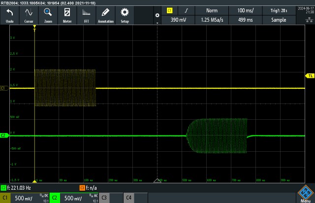
Here is how a 200Hz tone burst looks with a delay of 640 mSec:
MXR-113 Circuit Description
Here is a short description of some of the MXR-113 Delay circuitry.
Link to the original designer's web site:
The MXR-129 and 113 were designed by Tony Gambacurta. He talks about creating them here.
MXR-113 new memory board design:
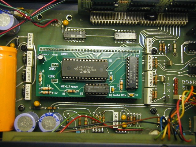
The owner of the MXR-113 that I was working on was interested in obtaining additional memory boards for his unit, as it only had one installed. At some point in the past it had all four boards, as evidenced by the label installed above the front panel delay switches. I found that the DRAM chips originally used were still available on line for about $10 each, so a new pcb could be populated for about $55 including the tantalum caps and IC sockets. But the DRAMs used were early 22-pin ones that did not multiplex the address inputs, which got me thinking that perhaps a different design using an SRAM chip might work. The memory boards each hold 4Kx5 bits, so a single 8K byte SRAM would be large enough. But then I decided that it would be even better to use a 32K byte SRAM and design one board that would replace all four of the original ones. Here is a photo of the prototype:
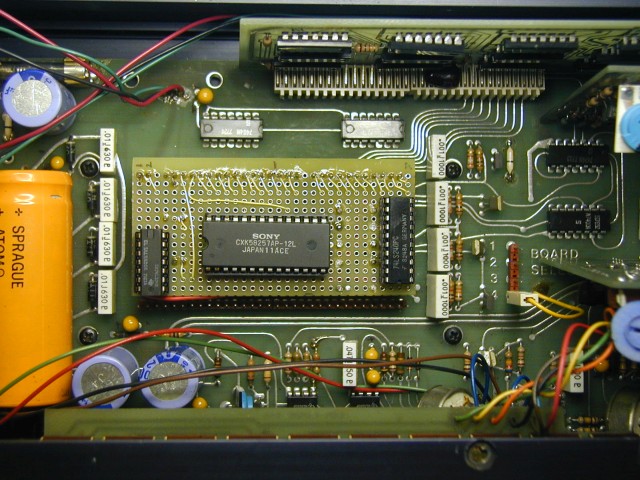
And here is a photo of the pcb version in place: